Introduction
Semiconductor Yield Management Software helps chip manufacturers, foundries, OSAT companies, fabless semiconductor firms, and process engineering teams monitor, analyze, and improve production yield. In simple words, it helps teams understand why some wafers, dies, or chips fail during manufacturing and what actions can improve output quality, reliability, and profitability.
Semiconductor manufacturing is highly complex. A small process variation, equipment issue, contamination event, design sensitivity, test pattern failure, or metrology drift can reduce yield and increase cost. Yield management software helps engineers collect data from wafer fabrication, inspection, metrology, test, assembly, and packaging systems, then analyze patterns to identify root causes faster.
These platforms are useful for defect analysis, wafer map analysis, process control, excursion detection, test data analysis, bin analysis, lot tracking, equipment correlation, advanced analytics, and cross-fab reporting. They help teams make better decisions by connecting manufacturing data, process data, product data, and test results.
Buyers should evaluate:
- Wafer map and defect analysis capability
- Integration with MES, SPC, metrology, inspection, and test systems
- Real-time analytics and excursion detection
- Root cause analysis workflows
- Support for fab, foundry, OSAT, and fabless workflows
- Data scalability and performance
- AI and machine learning support
- Reporting and dashboard flexibility
- Security, access control, and auditability
- Fit for high-volume semiconductor manufacturing
Best for: Semiconductor fabs, foundries, OSAT providers, fabless chip companies, process engineers, yield engineers, product engineers, quality teams, test engineers, data science teams, and manufacturing operations leaders.
Not ideal for: Very small electronics teams, basic PCB manufacturers, or companies that do not manage wafer-level, die-level, package-level, or semiconductor test data. In those cases, a general quality management tool, SPC tool, or BI platform may be enough.
Key Semiconductor Yield Management Software Trends
- AI-driven yield analytics is becoming more practical. Engineering teams are using machine learning to detect hidden process patterns, predict yield loss, and identify high-risk lots earlier.
- Wafer map analytics remains a core requirement. Engineers need fast visual analysis of die failures, spatial patterns, edge effects, cluster defects, and systematic yield problems.
- Real-time excursion detection is becoming more important. Fabs need alerts when process, equipment, or test data moves outside expected behavior.
- Cross-domain data correlation is now essential. Yield loss often requires connecting data from process tools, metrology, inspection, MES, test, design, and packaging.
- Advanced packaging is increasing data complexity. Chiplets, 3D packaging, heterogeneous integration, and complex assembly flows require stronger yield visibility across multiple manufacturing stages.
- Cloud and hybrid analytics models are growing. Some teams prefer cloud-scale analytics, while highly regulated or sensitive manufacturing environments may still need controlled or hybrid deployments.
- Fabless companies need better foundry and OSAT visibility. Fabless teams depend on external partners but still need strong yield reporting, test analytics, and product performance visibility.
- Data standardization is becoming a major challenge. Semiconductor teams must handle huge volumes of different data formats from tools, testers, MES, inspection systems, and engineering databases.
- Predictive quality is becoming a key goal. Instead of only reacting to yield loss, teams want to predict failures before they become large production problems.
- Security and IP protection are critical. Yield data may contain sensitive product, process, device, and customer information, so access control and data protection matter heavily.
How We Selected These Tools
The tools below were selected using a practical semiconductor manufacturing and engineering evaluation approach.
- Recognition in semiconductor manufacturing, yield management, process control, analytics, or test data analysis
- Ability to support wafer-level, die-level, lot-level, equipment-level, and product-level analysis
- Strength in defect analysis, wafer map visualization, root cause analysis, or production monitoring
- Fit for fabs, foundries, OSAT companies, fabless teams, or semiconductor engineering groups
- Integration potential with MES, SPC, metrology, inspection, test, and data platforms
- Support for high-volume manufacturing data and advanced analytics
- Ability to help engineering teams reduce yield loss and improve decision speed
- Practical usability for yield engineers, process engineers, product engineers, and quality teams
- Enterprise-readiness for security, governance, scalability, and support
- Fit across different company sizes and semiconductor operating models
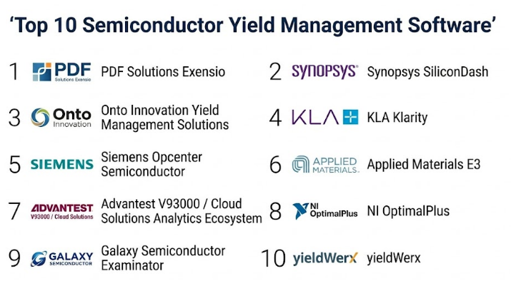
Top 10 Semiconductor Yield Management Software
#1 — PDF Solutions Exensio
Short description :
PDF Solutions Exensio is a semiconductor analytics and yield management platform designed for fabs, foundries, integrated device manufacturers, fabless companies, and OSATs. It helps engineering teams analyze manufacturing, test, process, and product data to improve yield and quality. The platform is known for supporting complex semiconductor data workflows across wafer fabrication, assembly, test, and product lifecycle stages. Exensio is useful when teams need deep visibility into yield loss, process variation, test results, and production behavior. It is a strong choice for organizations that need advanced analytics across the semiconductor value chain.
Key Features
- Semiconductor yield analytics
- Wafer map and die-level analysis
- Manufacturing and test data correlation
- Root cause analysis workflows
- Product and process performance tracking
- Advanced dashboards and reporting
- Support for fabless, foundry, and OSAT workflows
Pros
- Strong semiconductor-specific analytics depth
- Useful across manufacturing, test, and product engineering
- Good fit for complex high-volume environments
Cons
- May require implementation planning and data integration work
- Can be more advanced than smaller teams need
- Value depends heavily on data quality and engineering adoption
Platforms / Deployment
Web / Enterprise environment.
Cloud / Hybrid / Self-hosted: Varies / N/A.
Security & Compliance
Enterprise access controls may be available depending on deployment.
SSO/SAML, MFA, encryption, audit logs, RBAC: Not publicly stated in detail.
SOC 2, ISO 27001, GDPR, HIPAA: Not publicly stated.
Integrations & Ecosystem
Exensio is designed to work with complex semiconductor data environments where manufacturing, process, test, and product data need to be connected.
- MES and manufacturing data workflows
- Wafer sort and final test data
- Foundry and OSAT data sources
- Engineering analytics and dashboards
- API and data integration support: Varies / Not publicly stated
Support & Community
Support is generally enterprise-focused, with implementation assistance, technical support, and customer-specific onboarding. Community activity is more industry and customer-led than open public community based.
#2 — Synopsys SiliconDash
Short description :
Synopsys SiliconDash is a silicon lifecycle management and analytics platform that helps teams monitor semiconductor performance from design through manufacturing and field operation. It supports yield learning, silicon health monitoring, product analytics, and engineering decision-making. The platform is useful for semiconductor companies that want to connect design, manufacturing, test, and lifecycle data. SiliconDash is especially valuable when teams need visibility into how silicon behaves across different production and usage stages. It is a good fit for companies focused on improving product quality, yield learning, and long-term silicon performance.
Key Features
- Silicon lifecycle analytics
- Manufacturing and test data visibility
- Yield learning support
- Silicon health and performance monitoring
- Engineering dashboards
- Product behavior analysis
- Support for design-to-manufacturing feedback loops
Pros
- Strong connection between silicon lifecycle and analytics
- Useful for product engineering and yield learning
- Good fit for semiconductor companies managing complex chips
Cons
- May require strong data integration across teams
- Best suited for organizations with mature engineering workflows
- Pricing and detailed deployment information are not publicly simple
Platforms / Deployment
Web / Enterprise environment.
Cloud / Hybrid / Self-hosted: Varies / N/A.
Security & Compliance
Enterprise security controls may be available depending on deployment.
SSO/SAML, MFA, encryption, audit logs, RBAC: Not publicly stated in detail.
SOC 2, ISO 27001, GDPR, HIPAA: Not publicly stated.
Integrations & Ecosystem
SiliconDash fits into semiconductor engineering environments where design, test, manufacturing, and lifecycle data must be connected for better decision-making.
- Design-to-silicon analytics workflows
- Test and manufacturing data
- Product engineering dashboards
- Silicon lifecycle monitoring
- Integration availability: Varies / Not publicly stated
Support & Community
Support is generally enterprise-led through vendor documentation, customer support, technical teams, and implementation assistance. Community is mainly connected to the broader semiconductor design and EDA ecosystem.
#3 — Onto Innovation Yield Management Solutions
Short description :
Onto Innovation provides process control, inspection, metrology, and yield management solutions for semiconductor manufacturing. Its yield-related software helps teams analyze process variation, inspection results, metrology trends, and manufacturing issues. The platform is relevant for fabs and advanced packaging environments where inspection and measurement data play a major role in yield improvement. Onto Innovation is useful for teams that need to connect process control data with manufacturing decisions. It is a strong choice for organizations where defectivity, metrology, and process variation are key yield drivers.
Key Features
- Process control analytics
- Inspection and metrology data analysis
- Yield improvement workflows
- Defect and variation visibility
- Advanced packaging support
- Manufacturing analytics dashboards
- Equipment and process correlation support
Pros
- Strong connection to inspection and metrology workflows
- Useful for fabs and advanced packaging environments
- Helps engineers analyze process-driven yield issues
Cons
- May be most valuable when used with compatible process control environments
- Broader enterprise data integration may need planning
- Public details on security and deployment may be limited
Platforms / Deployment
Enterprise software environment.
Cloud / Self-hosted / Hybrid: Varies / N/A.
Security & Compliance
SSO/SAML, MFA, encryption, audit logs, RBAC: Not publicly stated in detail.
SOC 2, ISO 27001, GDPR, HIPAA: Not publicly stated.
Integrations & Ecosystem
Onto Innovation solutions fit strongly into semiconductor manufacturing environments where inspection, metrology, and process data need to support yield improvement.
- Inspection tool data
- Metrology data workflows
- Process control analytics
- Manufacturing dashboards
- Integration availability: Varies / Not publicly stated
Support & Community
Support is typically vendor-led and enterprise-focused. Implementation, training, and customer support may depend on the selected product modules and manufacturing environment.
#4 — KLA Klarity
Short description :
KLA Klarity is associated with semiconductor process control, defect management, yield analysis, and inspection data workflows. It supports engineering teams that need to analyze defects, classify patterns, investigate excursions, and improve process performance. KLA has strong relevance in semiconductor inspection and metrology, and Klarity fits well where yield challenges are connected to defectivity and process variation. The software is useful for fabs that need deep visibility into defect sources and manufacturing behavior. It is best suited for environments where inspection data is central to yield management.
Key Features
- Defect data analysis
- Process control and yield workflows
- Inspection data management
- Wafer-level defect visualization
- Excursion investigation support
- Pattern and trend analysis
- Manufacturing engineering dashboards
Pros
- Strong fit for defect-driven yield analysis
- Useful for fabs using inspection-heavy workflows
- Supports process engineering and yield teams
Cons
- May be more fab-focused than fabless-focused
- Best value may depend on inspection and metrology ecosystem fit
- Advanced workflows may need expert users
Platforms / Deployment
Enterprise software environment.
Cloud / Self-hosted / Hybrid: Varies / N/A.
Security & Compliance
Enterprise security options may be available depending on deployment.
SSO/SAML, MFA, encryption, audit logs, RBAC: Not publicly stated in detail.
SOC 2, ISO 27001, GDPR, HIPAA: Not publicly stated.
Integrations & Ecosystem
Klarity is relevant in environments where inspection, metrology, defect, and process data are central to yield improvement.
- Inspection data workflows
- Defect classification and analysis
- Wafer-level process data
- Manufacturing engineering analytics
- Integration availability: Varies / Not publicly stated
Support & Community
Support is generally enterprise-focused, with technical assistance, product documentation, and customer-specific support. Community activity is mostly industry and customer ecosystem based.
#5 — Siemens Opcenter Semiconductor
Short description :
Siemens Opcenter Semiconductor is a manufacturing operations solution designed for semiconductor production environments. While it is broader than yield management alone, it supports important manufacturing execution, production tracking, quality, and operational visibility workflows that affect yield. It is useful for fabs and semiconductor manufacturers that need strong MES-level control over lots, wafers, equipment, processes, and production routes. Yield teams can benefit from structured production data and traceability when analyzing process issues. It is a good fit for organizations that need manufacturing control and yield visibility together.
Key Features
- Semiconductor manufacturing execution support
- Lot and wafer tracking
- Production route management
- Process and equipment visibility
- Quality and manufacturing data capture
- Traceability support
- Enterprise manufacturing operations integration
Pros
- Strong fit for semiconductor manufacturing operations
- Useful for traceability and production control
- Supports yield improvement through better manufacturing data
Cons
- Not only a yield analytics platform
- Implementation can be complex for large fabs
- May require additional analytics tools for deep yield modeling
Platforms / Deployment
Enterprise software environment.
Cloud / Self-hosted / Hybrid: Varies / N/A.
Security & Compliance
Enterprise controls may be available depending on deployment.
SSO/SAML, MFA, encryption, audit logs, RBAC: Not publicly stated in detail.
SOC 2, ISO 27001, GDPR, HIPAA: Not publicly stated.
Integrations & Ecosystem
Opcenter Semiconductor fits into broader manufacturing operations and enterprise technology ecosystems.
- MES and shop-floor systems
- Equipment and process workflows
- Quality and traceability data
- Enterprise manufacturing integration
- Reporting and analytics tools
Support & Community
Support is enterprise-oriented, with implementation services, documentation, training, and technical support depending on the customer environment and deployment scope.
#6 — Applied Materials E3
Short description :
Applied Materials E3 is associated with equipment engineering, advanced process control, factory automation, and manufacturing analytics for semiconductor environments. It helps teams improve equipment performance, process stability, and factory-level decision-making. While not only a yield management platform, it supports yield improvement by helping engineers understand equipment behavior, process drift, and manufacturing performance. The platform is useful for fabs where equipment data and process control are central to production quality. It is best suited for teams that want to connect equipment intelligence with manufacturing outcomes.
Key Features
- Equipment engineering data analysis
- Process control support
- Factory automation workflows
- Manufacturing performance monitoring
- Equipment behavior analytics
- Process drift visibility
- Engineering decision support
Pros
- Strong relevance for equipment-heavy fab environments
- Helps connect process stability with yield outcomes
- Useful for advanced manufacturing control
Cons
- Not a simple standalone yield dashboard tool
- Best fit depends on fab systems and equipment environment
- Implementation may require strong engineering involvement
Platforms / Deployment
Enterprise software environment.
Cloud / Self-hosted / Hybrid: Varies / N/A.
Security & Compliance
SSO/SAML, MFA, encryption, audit logs, RBAC: Not publicly stated in detail.
SOC 2, ISO 27001, GDPR, HIPAA: Not publicly stated.
Integrations & Ecosystem
Applied Materials E3 is most relevant where equipment, process control, and fab automation data need to support manufacturing improvement.
- Equipment data workflows
- Factory automation systems
- Process control environments
- Engineering analytics
- Integration availability: Varies / Not publicly stated
Support & Community
Support is generally enterprise and fab-focused. Implementation and support needs depend on equipment ecosystem, factory architecture, and production workflows.
#7 — Advantest V93000 / Cloud Solutions Analytics Ecosystem
Short description :
Advantest is widely known for semiconductor test systems, and its analytics ecosystem supports test data analysis, yield learning, and production test optimization. It is useful for semiconductor companies that need to understand test results, bin patterns, device behavior, and production quality signals. While the core strength is closely related to test environments, test data is a major input for yield improvement and product engineering decisions. The platform ecosystem is especially useful for teams working with high-volume test data and product performance analysis. It is a strong fit where final test, wafer sort, and test engineering play a major role in yield learning.
Key Features
- Semiconductor test data analysis
- Wafer sort and final test visibility
- Bin and parametric data analysis
- Test program and production insights
- Product engineering analytics
- High-volume test data support
- Yield learning from test results
Pros
- Strong connection to semiconductor test workflows
- Useful for product and test engineering teams
- Helps improve visibility into device-level performance
Cons
- Most relevant when test data is the main analysis source
- May need integration with broader manufacturing data for full root cause analysis
- Platform scope may vary depending on implementation
Platforms / Deployment
Enterprise / test ecosystem environment.
Cloud / Hybrid / Self-hosted: Varies / N/A.
Security & Compliance
SSO/SAML, MFA, encryption, audit logs, RBAC: Not publicly stated in detail.
SOC 2, ISO 27001, GDPR, HIPAA: Not publicly stated.
Integrations & Ecosystem
Advantest analytics fits naturally into semiconductor test environments where device data, tester output, and production results need to be analyzed.
- Test data workflows
- Wafer sort and final test results
- Product engineering analysis
- Bin and parametric trend analysis
- Integration availability: Varies / Not publicly stated
Support & Community
Support is usually enterprise and customer-led, with technical services, documentation, and engineering support depending on the customer’s test environment.
#8 — NI OptimalPlus
Short description :
NI OptimalPlus is a semiconductor analytics platform focused on product analytics, test analytics, and manufacturing data intelligence. It helps teams analyze semiconductor production data, identify yield issues, improve quality, and support product engineering decisions. It is especially useful for companies that need to connect test data, manufacturing data, and product performance insights. OptimalPlus has strong relevance for fabless semiconductor companies, IDMs, and manufacturers that need product-level analytics across complex supply chains. It is a good choice when teams need visibility across outsourced manufacturing and test operations.
Key Features
- Semiconductor product analytics
- Test and manufacturing data analysis
- Yield and quality monitoring
- Supply chain visibility
- Product engineering dashboards
- Root cause analysis workflows
- High-volume data analytics
Pros
- Strong fit for fabless and product engineering teams
- Useful for outsourced semiconductor manufacturing visibility
- Helps connect test data with yield and quality outcomes
Cons
- May require strong data integration with external partners
- Best value depends on access to clean manufacturing and test data
- Deployment and pricing details are not publicly simple
Platforms / Deployment
Web / Enterprise analytics environment.
Cloud / Hybrid / Self-hosted: Varies / N/A.
Security & Compliance
Enterprise controls may be available depending on deployment.
SSO/SAML, MFA, encryption, audit logs, RBAC: Not publicly stated in detail.
SOC 2, ISO 27001, GDPR, HIPAA: Not publicly stated.
Integrations & Ecosystem
NI OptimalPlus fits into semiconductor data environments where product, test, and manufacturing data must be analyzed together.
- Test data sources
- Manufacturing partner data
- Product engineering dashboards
- Quality and reliability workflows
- Integration availability: Varies / Not publicly stated
Support & Community
Support is generally enterprise-focused, with technical support and implementation assistance depending on scope, data sources, and analytics needs.
#9 — Galaxy Semiconductor Examinator
Short description :
Galaxy Semiconductor Examinator is a semiconductor yield management and data analysis platform used for wafer map analysis, test data analysis, bin analysis, and yield reporting. It is useful for product engineers, test engineers, yield engineers, and fabless semiconductor teams that need practical analysis of production and test data. The platform helps users visualize wafer patterns, compare lots, identify trends, and investigate yield problems. Examinator is especially useful when teams need focused semiconductor analysis without building a custom analytics system from scratch. It is a practical choice for engineering groups that need strong wafer and test data visibility.
Key Features
- Wafer map analysis
- Test data analysis
- Bin analysis and visualization
- Yield reporting
- Lot and wafer comparison
- Product engineering workflows
- Failure pattern identification
Pros
- Strong focus on semiconductor yield and test analysis
- Useful for engineering teams needing practical wafer-level visibility
- Good fit for fabless and product engineering workflows
Cons
- May not cover full fab manufacturing operations
- Integration depth may depend on data formats and setup
- Security and compliance details are not fully public
Platforms / Deployment
Windows / Enterprise environment: Varies / N/A.
Cloud / Self-hosted / Hybrid: Varies / N/A.
Security & Compliance
SSO/SAML, MFA, encryption, audit logs, RBAC: Not publicly stated.
SOC 2, ISO 27001, GDPR, HIPAA: Not publicly stated.
Integrations & Ecosystem
Examinator is useful where wafer maps, test data, and yield reports need to be imported, visualized, and analyzed by engineering teams.
- Wafer map data
- Test result files
- Bin and parametric data
- Product engineering reports
- Integration availability: Varies / Not publicly stated
Support & Community
Support is vendor-led and focused on semiconductor engineering users. Public community visibility is limited, but the tool is relevant for specialized engineering analysis workflows.
#10 — yieldWerx
Short description :
yieldWerx is a semiconductor yield management and test data analytics platform designed to help engineering teams analyze wafer, lot, test, and production data. It supports yield improvement workflows by giving engineers visibility into failure patterns, bin distributions, process issues, and product behavior. The platform is useful for fabless companies, semiconductor manufacturers, and test engineering teams that need focused analytics for production yield. It helps reduce manual analysis effort and supports faster investigation of yield problems. yieldWerx is a practical option for teams that need semiconductor-specific analytics without relying only on generic BI tools.
Key Features
- Yield data analysis
- Wafer and lot-level analytics
- Test data visualization
- Bin analysis and reporting
- Failure pattern investigation
- Product engineering support
- Semiconductor-focused dashboards
Pros
- Designed specifically for semiconductor yield workflows
- Useful for test and product engineering teams
- Can reduce manual reporting and spreadsheet-based analysis
Cons
- May not cover full MES or fab operations management
- Advanced integrations may need implementation planning
- Public security and certification details are limited
Platforms / Deployment
Web / Enterprise environment: Varies / N/A.
Cloud / Self-hosted / Hybrid: Varies / N/A.
Security & Compliance
SSO/SAML, MFA, encryption, audit logs, RBAC: Not publicly stated.
SOC 2, ISO 27001, GDPR, HIPAA: Not publicly stated.
Integrations & Ecosystem
yieldWerx can support semiconductor engineering environments where test, wafer, lot, and product data need to be analyzed for yield improvement.
- Test data workflows
- Wafer and lot-level reporting
- Bin analysis
- Product and yield engineering dashboards
- Integration availability: Varies / Not publicly stated
Support & Community
Support is generally vendor-led and focused on semiconductor engineering teams. Documentation, onboarding, and support details may vary depending on deployment and customer requirements.
Comparison Table
| Tool Name | Best For | Platform(s) Supported | Deployment | Standout Feature | Public Rating |
|---|---|---|---|---|---|
| PDF Solutions Exensio | Enterprise semiconductor yield analytics | Web / Enterprise | Cloud / Hybrid / Varies | Cross-stage semiconductor analytics | N/A |
| Synopsys SiliconDash | Silicon lifecycle and product analytics | Web / Enterprise | Cloud / Hybrid / Varies | Design-to-silicon lifecycle visibility | N/A |
| Onto Innovation Yield Management Solutions | Process control and metrology-driven yield | Enterprise environment | Cloud / Hybrid / Varies | Inspection and metrology data analytics | N/A |
| KLA Klarity | Defect and inspection-based yield analysis | Enterprise environment | Cloud / Hybrid / Varies | Defect data and process control analysis | N/A |
| Siemens Opcenter Semiconductor | Semiconductor manufacturing operations | Enterprise environment | Cloud / Hybrid / Varies | MES-level production traceability | N/A |
| Applied Materials E3 | Equipment and process control analytics | Enterprise environment | Cloud / Hybrid / Varies | Equipment intelligence and process stability | N/A |
| Advantest Analytics Ecosystem | Semiconductor test data analytics | Enterprise / Test ecosystem | Cloud / Hybrid / Varies | Wafer sort and final test insights | N/A |
| NI OptimalPlus | Product and test analytics | Web / Enterprise | Cloud / Hybrid / Varies | Fabless supply chain yield visibility | N/A |
| Galaxy Semiconductor Examinator | Wafer map and test data analysis | Windows / Enterprise / Varies | Varies / N/A | Practical wafer map and bin analysis | N/A |
| yieldWerx | Semiconductor yield and test reporting | Web / Enterprise / Varies | Varies / N/A | Semiconductor-specific yield dashboards | N/A |
Evaluation & Semiconductor Yield Management Software
The scoring below is comparative and based on practical semiconductor buyer needs such as core yield features, ease of use, integration ecosystem, security signals, performance, support, and value. These scores should not be treated as final purchasing advice. The best platform depends on whether the buyer is a fab, foundry, OSAT, fabless company, IDM, or product engineering team.
| Tool Name | Core (25%) | Ease (15%) | Integrations (15%) | Security (10%) | Performance (10%) | Support (10%) | Value (15%) | Weighted Total (0–10) |
|---|---|---|---|---|---|---|---|---|
| PDF Solutions Exensio | 9 | 7 | 9 | 8 | 9 | 8 | 8 | 8.35 |
| Synopsys SiliconDash | 8 | 7 | 8 | 8 | 8 | 8 | 7 | 7.75 |
| Onto Innovation Yield Management Solutions | 8 | 7 | 8 | 7 | 8 | 8 | 7 | 7.60 |
| KLA Klarity | 8 | 7 | 8 | 7 | 9 | 8 | 7 | 7.70 |
| Siemens Opcenter Semiconductor | 8 | 7 | 9 | 8 | 9 | 8 | 7 | 8.00 |
| Applied Materials E3 | 8 | 7 | 8 | 7 | 9 | 8 | 7 | 7.70 |
| Advantest Analytics Ecosystem | 8 | 7 | 8 | 7 | 8 | 8 | 7 | 7.55 |
| NI OptimalPlus | 8 | 8 | 8 | 7 | 8 | 8 | 8 | 7.85 |
| Galaxy Semiconductor Examinator | 7 | 8 | 7 | 6 | 8 | 7 | 8 | 7.35 |
| yieldWerx | 7 | 8 | 7 | 6 | 8 | 7 | 8 | 7.35 |
A higher score usually means stronger overall fit across broad semiconductor yield requirements. However, a specialized tool may still be the right choice for a specific team. For example, a fab may prioritize inspection, metrology, MES, and equipment integration, while a fabless company may care more about test data analytics, OSAT reporting, and product-level yield visibility. Always test tools with real data before making a final decision.
Which Semiconductor Yield Management Software Should You Choose?
Solo / Freelancer
Solo consultants or independent semiconductor engineers usually do not need a large enterprise platform unless they are working with a client’s production data. They may need practical analysis tools for wafer maps, test data, and yield reports.
Good options:
- Galaxy Semiconductor Examinator for wafer map and test data review
- yieldWerx for focused yield and test analysis
- General BI or statistical tools for small data projects
The main goal should be fast analysis and clear reporting rather than complex enterprise integration.
SMB
Small semiconductor companies, early-stage fabless firms, and niche device makers often need focused yield visibility without heavy IT complexity. They may work with foundries, OSATs, and external test partners, so data import and reporting flexibility matter.
Good options:
- NI OptimalPlus for product and test analytics
- yieldWerx for focused yield analysis
- Galaxy Semiconductor Examinator for wafer map and bin analysis
- Synopsys SiliconDash if lifecycle visibility is important
SMBs should choose tools that reduce spreadsheet work, improve engineering speed, and support partner data workflows.
Mid-Market
Mid-market semiconductor companies often have multiple products, growing test data volume, more engineering teams, and stronger quality expectations. They need better correlation across lots, wafers, test results, suppliers, and product revisions.
Good options:
- PDF Solutions Exensio for advanced analytics
- NI OptimalPlus for product and manufacturing data visibility
- Synopsys SiliconDash for silicon lifecycle analytics
- Advantest analytics ecosystem for test-heavy workflows
- yieldWerx for practical yield reporting
Mid-market buyers should evaluate integration with foundry, OSAT, and internal engineering systems.
Enterprise
Large fabs, IDMs, foundries, and OSATs need highly scalable platforms that connect MES, process tools, inspection systems, metrology, test systems, product databases, and quality workflows. They also need strong governance, performance, and support.
Good options:
- PDF Solutions Exensio for enterprise semiconductor analytics
- Siemens Opcenter Semiconductor for manufacturing operations and traceability
- KLA Klarity for defect and inspection-driven yield analysis
- Applied Materials E3 for equipment and process control workflows
- Onto Innovation solutions for metrology and process analytics
- Synopsys SiliconDash for silicon lifecycle management
Enterprise buyers should involve process engineering, product engineering, IT, manufacturing operations, test, security, and data teams during selection.
Budget vs Premium
Budget-focused teams should start with focused tools that solve immediate pain points such as wafer map analysis, bin analysis, or test data reporting. They should avoid buying a large platform before defining clear use cases.
Premium platforms make more sense when the organization needs:
- Multi-site analytics
- Real-time excursion detection
- MES and equipment integration
- Advanced root cause analysis
- AI-assisted yield learning
- Strong governance and support
- High-volume manufacturing scalability
The right investment depends on the cost of yield loss, data complexity, and manufacturing scale.
Feature Depth vs Ease of Use
Feature-rich platforms can deliver deep value, but they may require expert setup, data engineering, integration work, and user training. Simpler tools can be adopted faster but may not solve complex fab-wide problems.
Choose feature depth when:
- Yield loss is expensive and complex
- Multiple data sources must be correlated
- Root cause analysis requires advanced analytics
- You need real-time monitoring
- You manage multiple fabs, products, or partners
Choose ease of use when:
- The team mainly needs wafer map review
- Test data analysis is the main requirement
- There is limited IT support
- Engineers need quick reports and visualizations
- Adoption speed matters more than enterprise governance
Integrations & Scalability
Semiconductor yield management depends heavily on data integration. A platform is only useful if it can consume, normalize, and analyze relevant data sources.
Important integration areas include:
- MES systems
- SPC systems
- Inspection tools
- Metrology tools
- Test systems
- Wafer sort data
- Final test data
- Equipment data
- Product databases
- Data lakes and BI platforms
- Foundry and OSAT partner data
- Quality and reliability systems
Scalability matters because semiconductor data can be extremely large. Buyers should test performance using realistic volumes of wafer, die, test, and process data.
Security & Compliance Needs
Semiconductor yield data can include sensitive process information, device performance, customer programs, production issues, and intellectual property. Security must be reviewed early in the buying process.
Buyers should ask vendors about:
- Role-based access control
- SSO and MFA
- Encryption
- Audit logs
- Data retention
- Backup and recovery
- Tenant isolation
- Access to sensitive customer or product data
- Secure file transfer
- Support for internal security reviews
Never assume a tool has a certification or compliance feature unless the vendor clearly confirms it.
Frequently Asked Questions
1. What is Semiconductor Yield Management Software?
Semiconductor Yield Management Software helps engineering teams monitor, analyze, and improve production yield across wafers, dies, lots, tests, and manufacturing processes. It helps identify why failures happen and where corrective action is needed.
2. Who uses Semiconductor Yield Management Software?
Yield engineers, product engineers, process engineers, test engineers, quality teams, fab operations teams, foundries, OSATs, IDMs, and fabless semiconductor companies use these tools to improve production performance and reduce yield loss.
3. How is yield management different from MES?
MES manages production execution, lot movement, process steps, and manufacturing traceability. Yield management focuses more on analyzing yield loss, defects, test failures, process variation, and root causes. Many companies need both.
4. What data does yield management software analyze?
It can analyze wafer maps, bin data, parametric test data, final test results, metrology data, inspection data, equipment data, process data, lot history, product information, and quality records.
5. Can yield management software reduce production cost?
Yes, it can help reduce cost by identifying yield loss earlier, reducing scrap, improving process stability, lowering rework, and helping teams act faster. However, results depend on data quality, engineering action, and process discipline.
6. What is the biggest mistake when choosing a yield platform?
The biggest mistake is choosing a tool without testing it on real semiconductor data. Demo data may look clean, but real production data can be messy, large, inconsistent, and difficult to correlate.
7. Is AI useful in semiconductor yield management?
Yes, AI can help detect patterns, predict yield risks, classify failures, identify abnormal behavior, and support root cause analysis. However, AI works best when data is clean, well-labeled, and supported by domain expertise.
8. Can fabless companies use yield management software?
Yes. Fabless companies often need yield analytics to monitor foundry data, OSAT data, wafer sort, final test results, product performance, and quality trends. Tools like NI OptimalPlus, PDF Solutions Exensio, Synopsys SiliconDash, yieldWerx, and Examinator may be relevant depending on needs.
9. How long does implementation take?
Implementation depends on data sources, data volume, integrations, user groups, security review, and workflow complexity. A focused test-data analytics setup may be faster, while a full enterprise fab deployment may require phased rollout.
10. What integrations are most important?
Important integrations include MES, SPC, metrology, inspection, test systems, equipment data, quality systems, data lakes, BI tools, and partner data feeds from foundries or OSATs. Integration quality can strongly affect platform value.
Conclusion
Semiconductor Yield Management Software is a critical part of modern chip manufacturing and product engineering because it helps teams understand yield loss, improve quality, reduce production cost, and make faster engineering decisions. The best tool depends on the company’s operating model. A fab may need strong MES, metrology, inspection, and equipment integration, while a fabless company may need test analytics, partner data visibility, and product-level yield dashboards. A large enterprise may require advanced analytics, governance, and multi-site scalability, while a smaller team may need focused wafer map and bin analysis. There is no single universal winner.